Op-Amp Electrical Specifications
In this article, "Op-Amp Electrical Specifications" will be explained in detail.
And the electrical specification parameters listed in the datasheet of the Analog Devices, Inc. are mainly used as reference.
What is the Electrical Specifications of an Op-Amp?
The op-amp electrical specifications are specifications that indicate the reall performance of the op-amp.
Since real op-amps are different from an ideal op-amp and contain various tolerance, we cannot select op-amps with laxity.
In order to select the best op-amp for the electronic circuit to be designed, it is necessary to read the datasheet and understand the op-amp electrical specifications.
Also, to understand the op-amp electrical specifications, it is better to know about an ideal op-amp beforehand.
Please refer to the following article for a detailed explanation.
For a more detailed explanation of the op-amp absolute maximum ratings, please refer to the following article.
Op-Amp Electrical Specifications
The parameters for op-amp electrical specifications are listed as shown below:
ELECTRICAL SPECIFICATIONS
| Parameter | DC Error | AC Error | DC/AC Error | Symbol | Unit |
|---|---|---|---|---|---|
| Input Offset Voltage | $V_{OS}$ | $V$ | |||
| Input Offset Voltage Drift | $ΔV_{OS}/ΔT$ | $V/℃$ | |||
| Input Bias Current | $I_B$ | $A$ | |||
| Input Bias Current Drift | $ΔI_B/ΔT$ | $I/℃$ | |||
| Input Offset Current | $I_{OS}$ | $A$ | |||
| Common-Mode Input Voltage Range | - | $V$ | |||
| Common-Mode Rejection Ratio | $CMRR$ | $dB$, $V/V$ | |||
| Open-loop Voltage Gain | $A_{OL}$ | $dB$, $V/V$ | |||
| Output Voltage Range | - | $V$ | |||
| Power Supply Rejection Ratio | $PSRR$ | $dB$, $V/V$ | |||
| Quiescent Current per amplifier | $I_Q$ | $A$ | |||
| Input Impedance | $Z_{IN}$ | $Ω$ | |||
| Output Impedance | $Z_{OUT}$ | $Ω$ | |||
| Frequency Response | - | - | |||
| Gain Bandwidth Product | $GBP$ | $Hz$ | |||
| Phase Margin | - | $deg$ | |||
| Gain Margin | - | $dB$ | |||
| Slew Rate | $SR$ | $V/sec$ | |||
| Settling Time | $t_s$ | $sec$ | |||
| Noise | - | - | |||
| Input Voltage Noise | $e_{n}p-p$ | $V_{p-p}$ | |||
| Input Voltage Noise Density | $e_n$ | $V/\sqrt{Hz}$ | |||
| Input Current Noise Density | $i_n$ | $A/\sqrt{Hz}$ |
*The "DC Error," "AC Error," and "DC/AC Error" related to the parameters are marked with ✔ (relevance "high"), respectively.
Input Offset Voltage
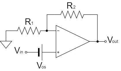
The input offset voltage $V_{OS}$ is the voltage discrepancy between the input + and input -.
As shown in the figure above, it is easy to understand the model as a non-inverting amplifier circuit of an ideal op-amp plus an offset voltage $V_{OS}$.
When $V_{out}$ is calculated, the error is added by the offset voltage $V_{OS}$ as shown below:
$$V_{out}=\left(1+\frac{R_2}{R_1}\right)V_{in}+\left(1+\frac{R_2}{R_1}\right)V_{OS}[V]$$
Therefore, the higher the gain, the greater the influence of the offset voltage $V_{OS}$ as an error.
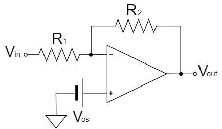
Similarly, in the inverting amplifier circuit, the output voltage with the offset voltage $V_{OS}$ added can be obtained as shown below:
$$V_{out}=\left(-\frac{R_2}{R_1}\right)V_{in}+\left(1+\frac{R_2}{R_1}\right)V_{OS}[V]$$
Input Offset Voltage Drift
The input offset voltage drift $ΔV_{os}/ΔT$ is the temperature drift of the input offset voltage $V_{os}$ due to temperature variation.
Input Bias Current
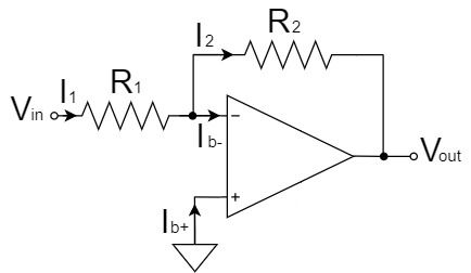
The input bias current $I_{B}$ is the current flowing into input + and input - of the op-amp, respectively.
In an ideal op-amp, the input bias current $I_{B}$ is 0, but in a real op-amp, the input bias current $I_{B}$ flows into the feedback resistor, resulting in an offset voltage.
(This offset voltage is a different parameter from the "input offset voltage" described earlier, so be careful not to confuse the two.)
For example, in an inverting amplifier circuit, the offset voltage due to the input bias current $I_{B}$ can be calculated as shown below:
$$I_1=\frac{V_{in}}{R_1}[A]$$
$$I_2=I_1-I_{B-}=\frac{V_{in}}{R_1}-I_{B-}[A]$$
$$V_{out}=-R_2I_2=-\frac{R_2}{R_1}V_{in}+R_2I_{B-}[V]$$
This indicates that the offset voltage of $R_2I_{B-}$ is an error factor, and the larger the value of the feedback resistor $R_2$, the greater the effect.
For an inverting amplifier circuit, the bias current $I_{B}$ can also be canceled by connecting a bias compensation resistor in series with Input + to generate an offset voltage.
However, since $I_{B+}$ and $I_{B-}$ are not exactly the same value, the difference is the "input offset current $I_{OS}$".
Input Bias Current Drift
The input bias current drift $ΔI_{B}/ΔT$ is the temperature drift of the input bias current due to temperature variation.
Input Offset Current
As explained in "Input Bias Current," the bias currents $I_{B+}$ and $I_{B-}$ are not exactly the same value, so even if the bias current $I_{B}$ is cancelled, the difference is the "input offset current $I_{OS}$.
The input bias current $I_{B}$ becomes smaller than the input bias current $I_{B}$, but the input offset current $I_{OS}$ flows through the feedback resistor of the op-amp, which generates an offset voltage and becomes an error factor.
In the case of an inverting amplifier circuit, the calculation can be done as shown below:
$$I_{OS}=|I_{B+}-I_{B-}|[A]$$
$$V_{out}=-\frac{R_2}{R_1}V_{in}+R_2I_{OS}[V]$$
Common-Mode Input Voltage Range
The common-mode input voltage range is the range of voltages that can be input to an op-amp. It may be simply stated in the datasheet as "Input Voltage Range".
In particular, if the input or output can be as wide as the supply voltage range of the op-amp, it is called a "Rail-to-Rail Op-Amp".
For example, if the power supply of an op-amp is ±15 V, a rail-to-rail op-amp can input or output up to ±15 V, just like the power supply.
However, since it varies depending on the op-amp, such as "rail-to-rail for both input and output," "rail-to-rail for output only," etc., be sure to check the "output voltage range" carefully in the datasheet.
Common-Mode Rejection Ratio
The common-mode rejection ratio (CMRR) is the ability of an op-amp to remove the fluctuations (ripples) of common-mode input voltage. It is a particularly important parameter in differential amplifier circuits.
If the fluctuations of the common-mode input voltage of the op-amp is $ΔV_{CM}$ and the fluctuations of the input offset voltage of the op-amp is $ΔV_{OS}$, it can be defined as shown below:
$$CMRR=\frac{ΔV_{CM}}{ΔV_{OS}}[V/V] \quad or \quad CMRR=20log\frac{ΔV_{CM}}{ΔV_{OS}}[dB]$$
From this equation, it can be seen that the smaller the input offset voltage fluctuations are for a given common-mode input voltage fluctuations, the larger the common-mode rejection ratio (CMRR) will be.
If the differential voltage gain of the op-amp is $A_d$ and the common-mode voltage gain of the op-amp is $A_c$, it can also be defined as shown below:
$$CMRR=\frac{A_d}{A_c}[V/V] \quad or \quad CMRR=20log\frac{A_d}{A_c}[dB]$$
From the equation, it can be seen that the smaller the common-mode voltage gain compared to the differential voltage gain, the larger the common-mode rejection ratio (CMRR).
Therefore, if the common-mode rejection ratio (CMRR) is large, common-mode noise can be eliminated in the op-amp differential amplifier circuit.
However, the resistance tolerance of the differential amplifier circuit will affect the value of the common-mode rejection ratio (CMRR).
Open-loop Voltage Gain
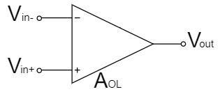
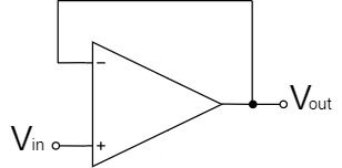
The open-loop voltage gain $A_{OL}$ is the gain when a DC differential voltage $V_{in+}-V_{in-}$ is applied to the op-amp with no negative feedback (open) as shown in the above figure.
(Since a large signal of 1V or more is added, it may be described in the datasheet as a large signal voltage gain $A_{VO}$.)
And the open-loop Voltage Gain $A_{OL}$ is:
$$A_{OL}=\frac{V_{out}}{V_{in+}-V_{in-}}[V/V] \quad or \quad A_{OL}=20log\frac{V_{out}}{V_{in+}-V_{in-}}[dB]$$
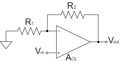
Now, as an example, consider how the open-loop voltage gain affects the amplification factor of a non-inverting amplifier circuit.
$$V_{out}=\left(1+\frac{R_2}{R_1}\right)V_{in} \times \frac{1}{1+\left(1+\frac{R_2}{R_1}\right)\frac{1}{A_{OL}}}[V]$$
For an ideal op-amp, the open-loop voltage gain is $A_{OL}=∞$, so the amplification factor of the non-inverting amplifier circuit is not affected.
$$V_{out}=\left(1+\frac{R_2}{R_1}\right)V_{in} \times \frac{1}{1+\left(1+\frac{R_2}{R_1}\right)\frac{1}{∞}}=\left(1+\frac{R_2}{R_1}\right)V_{in}[V]$$
However, the open-loop voltage gain of a real op-amp is limited. If $R_1=1[kΩ]$, $R_1=10[kΩ]$, and $A_{OL}=80[dB] (10000x)$, the amplification factor obtained in a non-inverting amplifier circuit is:
$$V_{out}=(11)V_{in} \times \frac{1}{1+(11)\frac{1}{10000}}=\frac{11}{1.0011}V_{in}≒10.988V_{in}$$
It is smaller than the amplification factor of 11 times that obtained by the non-inverting amplifier circuit of an ideal op-amp, and the difference is called the "gain error".
The difference between "Large Signal" and "Small Signal" as described in the datasheets of the op-amp is the magnitude of the signal voltage.
Although not clearly defined, it seems that large signals should be 1V or higher and small signals should be 200mV or lower.
Output Voltage Range
The output voltage range is the range of voltage that the op-amp can output. It may be described as "Output Voltage High" or "Output Voltage Low" in the datasheet.
As explained in "Common-Mode Input Voltage Range," if the input or output can be as wide as the supply voltage range of the op-amp, it is called a "Rail-to-Rail Op-Amp".
However, since it varies depending on the op-amp, such as "rail-to-rail for both input and output," "rail-to-rail for output only," etc., be sure to check the "common-mode input voltage range" carefully in the datasheet.
Power Supply Rejection Ratio
The power supply rejection ratio (PSRR) is the ability to remove fluctuations (ripples) in the voltage input to the power supply pins of an op-amp.
If the fluctuations of the supply voltage for the op-amp is $ΔV_S$ and the fluctuations of the input offset voltage for the op-amp is $ΔV_{OS}$, it can be defined as shown below:
$$PSRR=\frac{ΔV_S}{ΔV_{OS}}[V/V] \quad or \quad PSRR=20log\frac{ΔV_S}{ΔV_{OS}}[dB]$$
For example, if $PSRR=100[dB]=10^5$ and $ΔV_S=10[V]$;
$$ΔV_{OS}=\frac{ΔV_S}{PSRR}=\frac{10}{10^5}=10[uV]$$
Therefore, amplifying 100x with an op-amp will result in $1[mV]$ fluctuations in output voltage.
Quiescent Current per amplifier
The quiescent current is the current consumed by an op-amp when only power is applied to it and no input signal or load current is flowing (quiescent state).
In datasheets, quiescent current is often listed in "per amp".
Input Impedance
The input impedance of a real op-amp is $10^{6}[Ω]$ to $10^{9}[Ω]$.
(The ideal op-amp is $∞[Ω]$.)
The input impedance of the non-inverting amplifier circuit is approximately equal to the input impedance of the op-amp, while the input impedance of the inverting amplifier circuit is the value of the input resistor connected to input -.
However, even with a non-inverting amplifier circuit, any input impedance can be set by connecting a resistor to input + and GND.
Output Impedance
The output impedance of a real op-amp is $10^{2}[Ω]$.
(The ideal op-amp is $0[Ω]$.)
However, in the case of circuits with negative feedback, such as inverting and non-inverting amplifier circuits, the voltage drop caused by the output impedance is compensated, so the output impedance can be considered as almost $0[Ω]$.
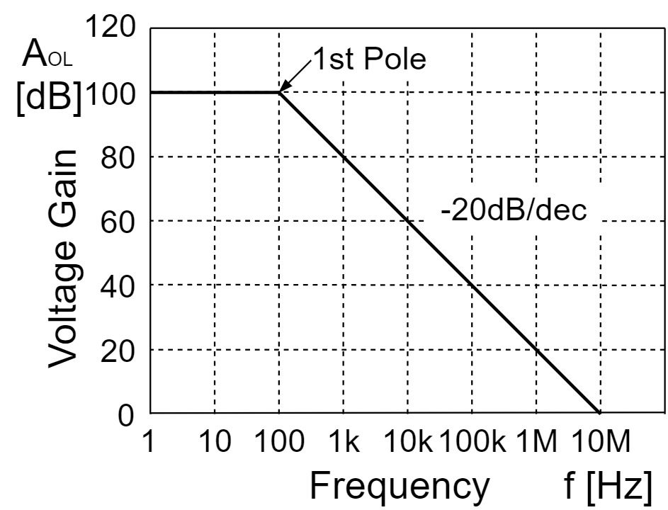
Frequency Response
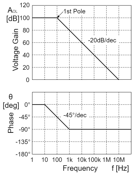
The frequency response of an op-amp is generally the frequency response of "open-loop voltage gain $A_{OL}$" and "phase $θ$".
In an ideal op-amp, the gain is constant over the entire frequency band, but in a real op-amp, the gain decreases with a slope of $-20[dB/dec](-6[dB/oct])$ from a certain frequency.
The frequency at which the gain begins to decrease is called the "pole," and the frequency at which the gain is $0[dB]$ (1x) is called the "unity gain frequency $f_T$".
On the other hand, the phase begins to delay at 1/10th the frequency of the pole and is $-45°$ at the pole frequency, $-90°$ at 10 times the pole frequency, and then remains constant.
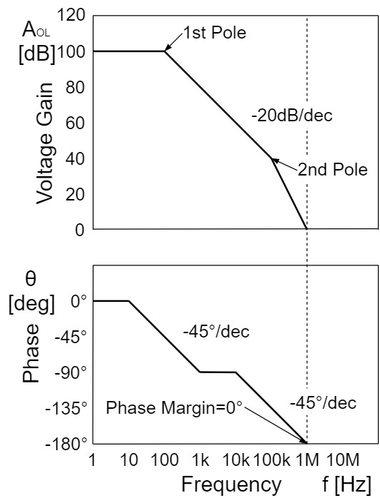
Also, the frequency response shown in the above figure is for a fully compensated op-amp, while a uncompensated op-amp would have a frequency response with two poles, 1st pole and 2nd pole, as shown below:
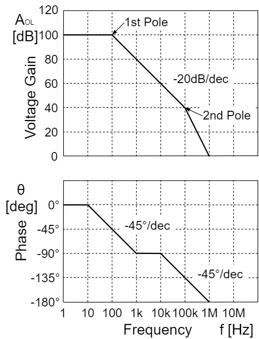
In this case, at the 2nd pole, the gain attenuation is $-40[dB/dec](-12[dB/oct])$ and the phase is further delayed by $-45°$ at the 2nd pole frequency and $-90°$ at 10 times the pole frequency. Thus, the phase delay reaches a maximum of $-180°$.
If the phase of the op-amp is delayed by $-180°$, the negative feedback is inverted and changed to the positive feedback, resulting in oscillation.
A fully compensated op-amp usually does not oscillate because the phase delay is constant at $-90°$.
However, if a capacitor etc. is connected to the inverting input or output of the op-amp, the possibility of oscillation increases due to the phase delay caused by the CR integrator circuit.
*At the pole frequency, it attenuates by $-3[dB/dec]$ like a 1st-order low-pass filter, but this is omitted in the frequency response figure in this article.
Fully compensated op-amps are resistant to oscillation, but at the expense of GB product, so they cannot operate with high gain or at high frequencies.
Uncompensated op-amps are vulnerable to oscillation, but can operate with high gain and high frequency due to their large GB product.
Gain Bandwidth Product(GBW)
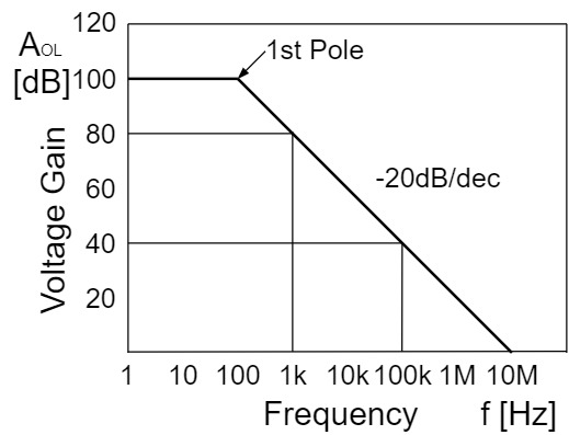
The gain bandwidth product $GBW$ is the product of an arbitrary frequency and amplification factor in the region of attenuation at $-20[dB/dec]$ for a fully compensated op-amp.
If the frequency $f[Hz]$ and the amplification factor $A[times]$, the equation with the gain bandwidth product $GBW$ is:
$$GBW=fA[Hz]$$
For example, $GBW_1$ for $f=1[kHz]$ and $A=80[dB]=10000[times]$ and $GBW_2$ for $f=100[kHz]$ and $A=80[dB]=100[times]$, respectively, are obtained as shown below:
$$GBW_1=fA=1\times10^3\times10000=10\times10^6=10[MHz]$$
$$GBW_2=fA=100\times10^3\times100=10\times10^6=10[MHz]$$
$$GBW_1=GBW_2$$
This shows that the gain bandwidth product $GBW$ is always constant in the region of attenuation at $-20[dB/dec]$.
Therefore, the op-amp with a larger gain-bandwidth product $GBW$ can stably amplify up to higher frequency bands.
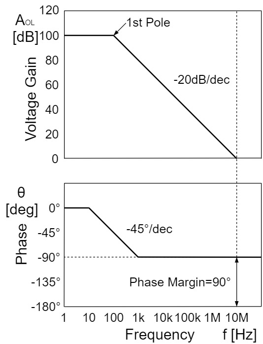
Phase Margin
The phase margin indicates how much phase margin is available from $-180°$ at a frequency with a gain of $0[dB]$.
In a normal op-amp, the phase is designed at about $45~60°$ and is used as an oscillation margin as well as a gain margin.
For example, the following figure shows a phase margin of $90°$, which is sufficient phase margin and will not oscillate in normal use.
Also, in the figure below, the phase margin is $0°$, so the negative feedback is inverted to become positive feedback and oscillation occurs.
Gain Margin
The gain margin indicates how much margin the gain has from $0[dB]$ at a frequency with a phase of $-180°$.
In a normal op-amp, it is designed at about $-7~-10[dB]$ and is used as an oscillation margin as well as a phase margin.
Slew Rate
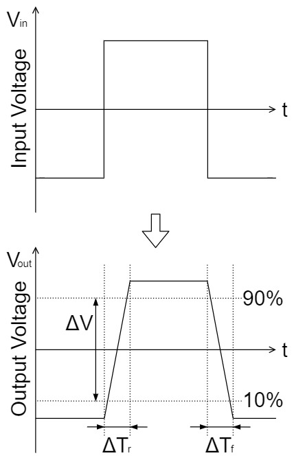
The slew rate $SR$ is the operating speed of the op-amp. It is the rate at which the output voltage of an op-amp can change per constant unit time.
$$SR=\frac{ΔV}{ΔT}[V/s]$$
Also, the slew rate $SR$ may be divided into rising time $ΔT_r$ and falling time $ΔT_f$, as shown below:
$$SR_r=\frac{ΔV}{ΔT_r}[V/s] \quad SR_f=\frac{ΔV}{ΔT_f}[V/s]$$
A real op-amp is limited by a slew rate of $SR$.
Therefore, when a square wave with a sudden change in rise and fall is input to an operational amplifier, the output voltage cannot follow and the square wave is distorted into a trapezoidal shape.
In addition, for sine waves, if the frequency is high enough, the output voltage cannot follow and the waveform is distorted into a triangular wave.
Here, the frequency at which a voltage follower circuit with an amplification factor of 1x can output is obtained as shown below:
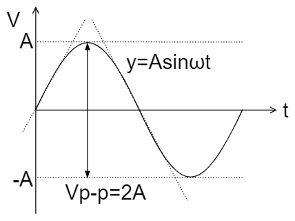

$$y=Asinωt$$
Since the slew rate $SR$ is the slope of the tangent line of the sine wave, the above equation $y$ is differentiated.
$$\frac{dy}{dt}=Aωcosωt, \quad ωt=0$$
Thus, since $ω=2πf, V_{p-p}=2A$, the slew rate $SR$ is:
$$SR=\frac{dy}{dt}=Aωcosωt=Aωcos0=Aω=2πfA=πfV_{p-p}[V/s]$$
Furthermore, the frequency $f$ and voltage amplitude $V_{p-p}$ are:
$$f=\frac{SR}{πV_{p-p}}[Hz], \quad V_{p-p}=\frac{SR}{πf}[V]$$
Therefore, the larger the slew rate $SR$ and the smaller the voltage amplitude, the higher the frequency that can be output.
For example, when $SR=50[V/us]=50\times10^{6}[V/s]$ and $V_{p-p}=1[V]$, the possible output frequency is:
$$f=\frac{SR}{πV_{p-p}}=\frac{50\times10^{6}}{π\times1}≒15.9[MHz]$$
If the amplification factor $A_V$ is added, such as in non-inverting or inverting amplifier circuits:
$$f=\frac{SR}{πV_{p-p}A_V}[Hz], \quad V_{p-p}=\frac{SR}{πfA_V}[V]$$
From the above equation, the larger the amplification factor, the lower the frequency at which output is possible.
For example, when $SR=50[V/us]=50\times10^{6}[V/s]$, $V_{p-p}=1[V]$, and $A_{V}=10[times]$, the possible output frequencie is:
$$f=\frac{SR}{πV_{p-p}A_V}=\frac{50\times10^{6}}{π\times1\times10}≒1.59[MHz]$$
As the amplification factor $A_V$ increases from 1x to 10x, the available output frequency decreases by 1/10.
Settling Time
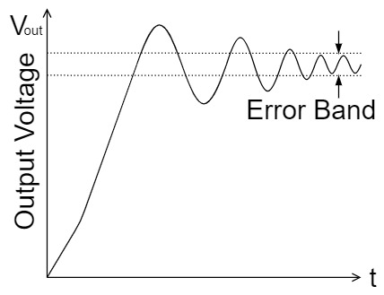
Settling time $t_s$ is the time it takes for the output to fall within a certain error range when a step input is applied to the op-amp.
The step input is a pulse of rapidly rising voltage, which causes the output voltage to be trapezoidal or the fluctuations of the voltage, called ringing, depending on the slew rate.
If the settling time $t_s$ is short, it means that these phenomena have a short time to converge.
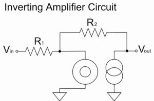
Noise
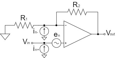
Focusing on the voltage and current noise of op-amps, we will consider the noise model connected to the non-inverting amplifier circuit of an ideal op-amp, as shown in the figure above.
The voltage noise and the current noise include "1/f noise" in the low frequency band and "white noise" in the high frequency band as shown below:
(There are other types of noise, but they are omitted in this article.)
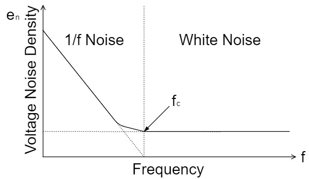
The "1/f noise" increases inversely $3[dB/oct]$ from the corner frequency $f_c$, while the "white noise" remains constant.
Also, as units of noise, the voltage noise density $e_n$ is $V/\sqrt{Hz}$ and the current noise density $i_n$ is $A/\sqrt{Hz}$.
Input Voltage Noise
The input voltage noise $e_{n}p-p$ may be expressed in units of "$V_{p-p}$" in a limited frequency bandwidth (e.g. 0.1 to 10 Hz), especially as an indicator of "1/f noise".
Input Voltage Noise Density
The input voltage noise density $e_n$ can be expressed in units of "$V/\sqrt{Hz}$" to calculate the input voltage noise $V_n$ at a particular frequency.
For example, if $e_n=5[nV/\sqrt{Hz}]$ and $f=100[kHz]$;
$$V_n=e_n\times\sqrt{f}=5\times\sqrt{100\times1000}=1581[nV]$$
Also, if $e_n=5[nV/\sqrt{Hz}]$ and $f=1000[kHz]$;
$$V_n=e_n\times\sqrt{f}=5\times\sqrt{1000\times1000}=5000[nV]$$
Suppose the input voltage noise $V_n$ is high, it will be amplified by the op-amp as it is, so that a weak input signal will be buried in the noise.
Input Current Noise Density
The input current noise density $i_n$ is expressed in units of "$A/\sqrt{Hz}$.
Since it is difficult to understand the current value as it is, this input current noise density $i_n$ is converted to input voltage noise density and summed with the input voltage noise density $e_n$.
If $i_n=i_{n+}=i_{n-}$, then the input voltage noise $V_n$, the sum of the input voltage noise density $e_n$ and the input current noise density $i_n$, is:
$$V_n=\sqrt{e_n^2+\left(\frac{R_1R_2}{R_1+R_2}\right)^2i_n^2}[V]$$
The input current noise density $i_n$ is affected by the external resistance of the op-amp, and higher resistances result in higher noise.
However, while the input voltage noise density $e_n$ is on the order of "$nV/\sqrt{Hz}$($10^{-9}$), the input current However, the input voltage noise density $e_n$ is on the order of "$nV/\sqrt{Hz}$($10^{-9}$)", while the input current noise density $i_n$ is very small, on the order of "$fA/\sqrt{Hz}$($10^{-15}$)", so it can be ignored.